Tutorial for RAIL Library Getting Started
Author:Chixiao Chen
This is a simple tutorial of how to implement a RAIL flow to design an AMS module from scratch to a LVS/DRC clean GDS. To elaborate the idea of RAIL, we illustrate the entire flow step by step, rather than providing a fully automatic makefile-based flow.
Before getting started, we need to download and unzip the following files from RAIL/rail65 repo to your VLSI design server.
- analog/cdk_oa/rail.zip cds.lib
- digital/front_end/rail65.db
- digital/backe_end/FRAM_only/rail65.zip
- analog/gds/rail65.gds (This file is not open for download due to confidentiality agreement, please contact rail4open@gmail.com).
This tutorial uses Cadence IC6, Synopsys ICC and Mentor Calibre to complete the example.
Step 1: Load a Verilog Netlist
In this example, we are going to design a CMOS transmission gate whose turn-on resistance is less than 200 Ohm at 0.6V bias point. We are going to use the RAIL cell, TGAT, and some digital gates from standard cell library. The RAIL compiler will generate a verilog-based netlist as follow,
// File: swbk01.v
`timescale 1ns/1ps
module SW_BANK_01 (
  input  SW,
  output POS, NEG
  );
  BUFFD3 b01  (.I(SW),.Z(SWB));
  TGAT   sw00 (.SW(SWB),.POS(POS),.NEG(NEG));
  TGAT   sw01 (.SW(SWB),.POS(POS),.NEG(NEG));
  TGAT   sw02 (.SW(SWB),.POS(POS),.NEG(NEG));
  TGAT   sw03 (.SW(SWB),.POS(POS),.NEG(NEG));
  TGAT   sw04 (.SW(SWB),.POS(POS),.NEG(NEG));
  TGAT   sw05 (.SW(SWB),.POS(POS),.NEG(NEG));
endmodule
The top cell named as SW_BANK_01 is composed by 6 TGAT cells connected in parallel, which are driven by BUFFD3 from standard library. This verilog file can be found under the RAIL repo, rail65/sample_getting_started.
Step 2: Generate an OA-based Schematic
Modify power supply ports of the netlist,
// File: swbk01_sch.v
`timescale 1ns/1ps
module SW_BANK_01 (
  inout  VDD,VSS,  // Power supply ports
  input  SW,
  output POS, NEG
  );
  BUFFD3 b01  (.I(SW),.Z(SWB), .VDD(VDD),.VSS(VSS));
  TGAT   sw00 (.SW(SWB),.POS(POS),.NEG(NEG), .VDD(VDD),.VSS(VSS));
  TGAT   sw01 (.SW(SWB),.POS(POS),.NEG(NEG), .VDD(VDD),.VSS(VSS));
  TGAT   sw02 (.SW(SWB),.POS(POS),.NEG(NEG), .VDD(VDD),.VSS(VSS));
  TGAT   sw03 (.SW(SWB),.POS(POS),.NEG(NEG), .VDD(VDD),.VSS(VSS));
  TGAT   sw04 (.SW(SWB),.POS(POS),.NEG(NEG), .VDD(VDD),.VSS(VSS));
  TGAT   sw05 (.SW(SWB),.POS(POS),.NEG(NEG), .VDD(VDD),.VSS(VSS));
endmodule
Before launching the virtuoso, make sure cds.lib has been configured correctly so that rail65/tsmcN65/tcbn65lp/analogLib/basic can be found in your library manager.
Launch Virtuoso, and create a libary named as rail_design or any name you like.
Then we import the netlist to construct a schematic view for SW_BANK_01.
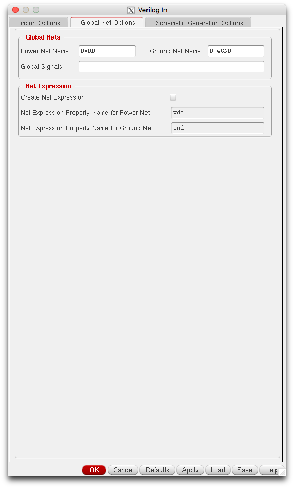
File –> Import –> Verilog, configure the VerilogIn as follows,

Then we add the verilog netlist to the library you created, and also include the reference library of basic/tcbn65lp(standard cell)/rail65. To avoid conflict with global pin, we recommend using a name different from your power/gound pin, as shown below
Click OK or Apply. Virtuoso supports a structual verilog schematic generation. If verilog imports successfully, you will see a new schematic in the rail_design library.

The generated schematic can be used for pre-layout simulation and LVS.
Step 3: Generate a Milkyway-based Physcal Design
Now we are ready to create the transmission gate layout by the digital flow. In the example, we are using IC Compiler from Synopsys.
First, let us config all the path needed in the 0_def.tcl file.
# File: 0_def.tcl
# The milkyway lib path and input/output path
set LIBR_PATH mw_proj/rail_getting_start
set RTL_PATH    rtl/swbk01.v
set MODULE_NAME SW_BANK_01
set VERSION     _v1
set GDS_PATH aprout/$MODULE_NAME$VERSION.gds
...
# The backend files provided by foundry and RAIL project
set TECHFILE_PATH  /.../tsmcn65_9lmT2.tf
set STDCELL_DB_PATH /.../tcbn65lp_200a
set RAILIB_DB_PATH /../digital/front_end/ # where rail65.db is stored
....
# The physical information set, including floorplan area and allowed routing metal
set TILE_HT 1.8
set TILE_WD 0.2
set CORE_ROW 7
set CORE_COL 39
set CORE_HT [expr {$TILE_HT * $CORE_ROW}]
set CORE_WD [expr {$TILE_WD * $CORE_COL}]
set TOP_RT_METAL M5
Second, we create the target design based the verilog list we obtained in step 1. The key steps include
# File: 1_create.tcl
# Create the library, if already exist can open it
create_mw_lib \
-technology $TECHFILE_PATH \
-mw_reference_library $REFLIB_PATH \
-open $LIBR_PATH
...
# Import the Verilog and create the floorplan
read_verilog -top $MODULE_NAME -allow_black_box $RTL_PATH
create_floorplan -control_type width_and_height \
-core_width $CORE_WD \
-core_height $CORE_HT \
-bottom_io2core 0.1 -top_io2core 0.1 -left_io2core 0.2
...
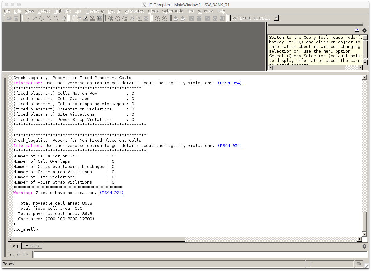
# First Check
check_legality
If the definition works all good, the results of check_legality should have no error, like the screenshot below
The next step is placement and routing. In the case, we mark all the steps explicitly. Note that the power supply and analog nets are routed manually due to their parasitic sensitivity, but the digital nets are done automatically as,
# File: 2_place_route.tcl
...
# This part routing the power and analog manually
create_power_straps  -direction vertical  -start_at 0.700 -nets  {VSS}  -layer M2 -width 0.3 -look_inside_std_cell
...
# This part routes the digital signal automatically
set_route_mode_options -zroute true
...
route_zrt_detail
...
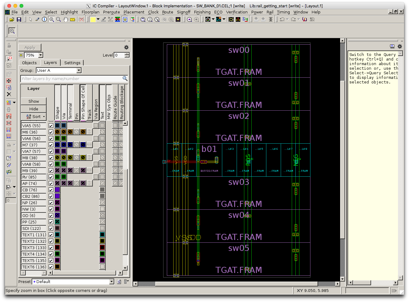
A screenshot is illustrated below for a successful placement and routing.
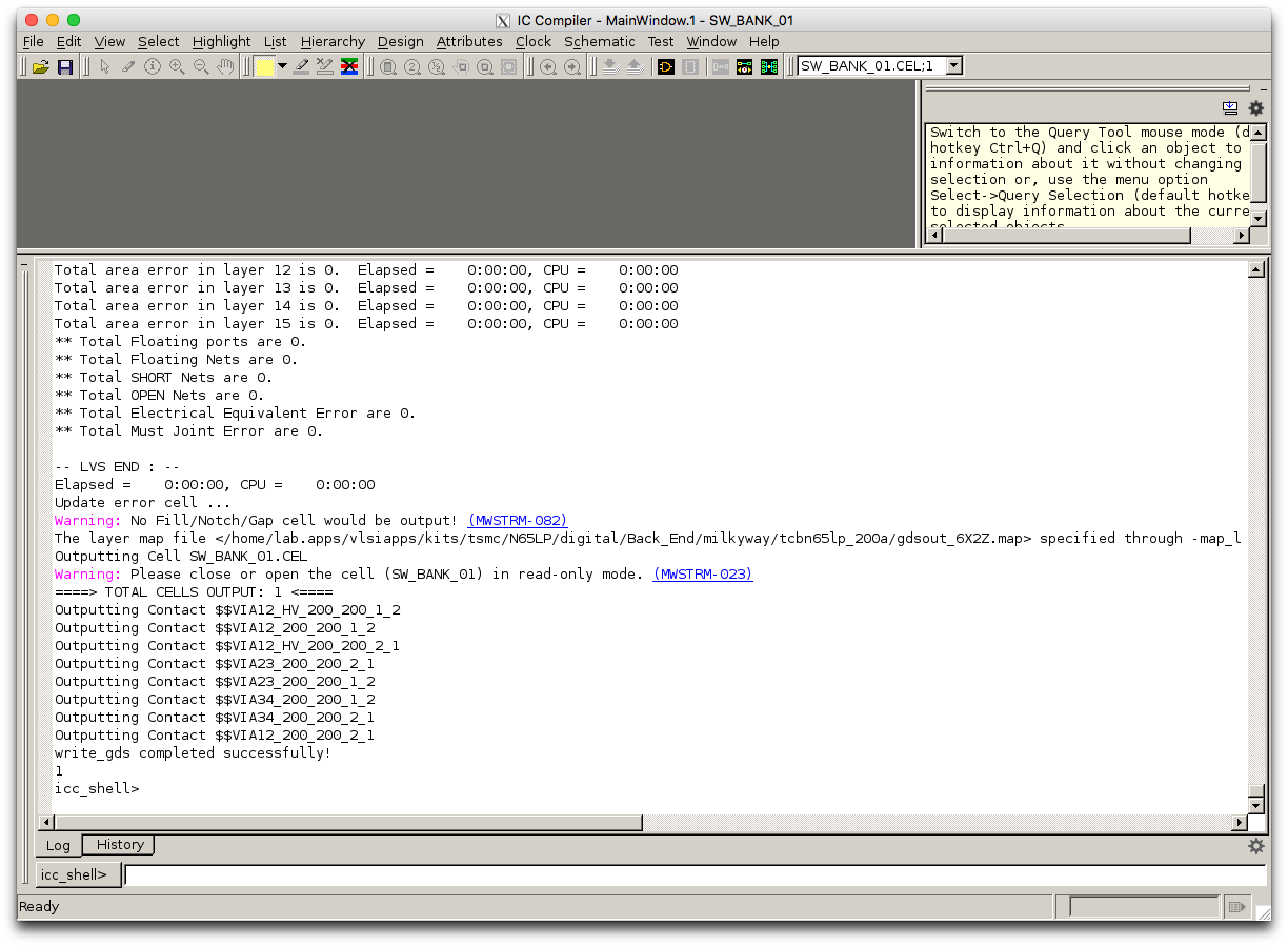
To complete the layout, we will do LVS check in ICC. There should be no erros in this sample. After that, the layout is going to be exported in GDS format. The script looks like,
# File: 3_signoff.tcl
...
# Verify the placement and routing
verify_lvs
# Export the GDS-II file
set_write_stream_options -child_depth 0 -skip_ref_lib_cells \
                         -map_layer $MAP_PATH
write_stream -format gds -cells  $MODULE_NAME $GDS_PATH
...
The screenshot of these steps is shown below.
All the script metioned in the step is avaialbe in the rail65 repo, under the directory of sample_getting_started.
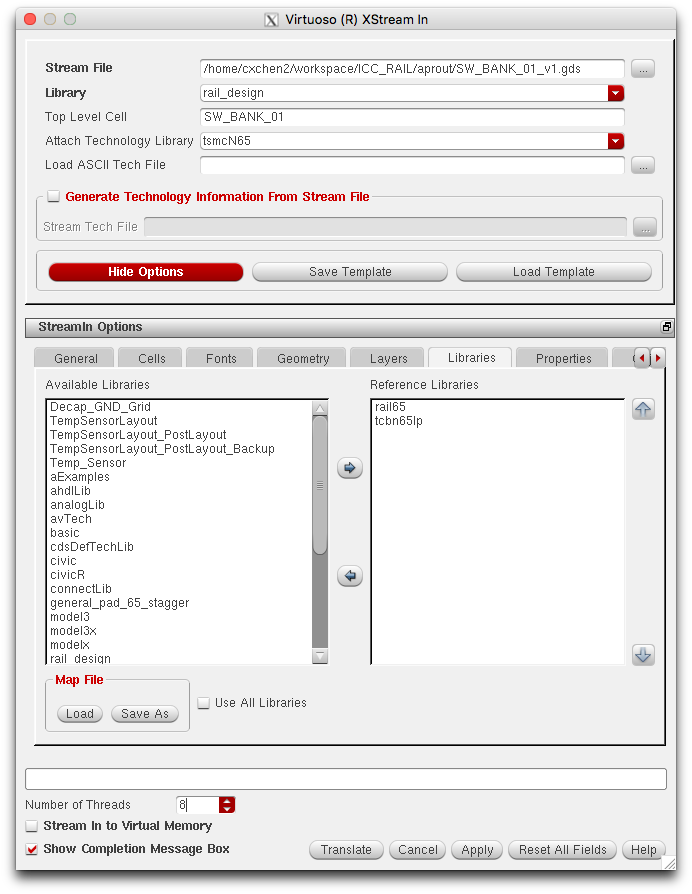
Step 4: Merge the GDS and Import to Virtuoso
If your rail65.gds is seperate from the OA database in Virtuoso, you can use calibredrv to merge the gds
calibredrv -a layout filemerge -in SW_BANK_01_v1.gds -indir /../analog/gds -out SW_BANK_01_m1.gds -topcell SW_BANK_01
But we highly recommend streaming-in the rail65.gds file to the rail65 library in virtuoso first. After that, you do not need to do the gds merge. The following figure shows the stream-in flow in the virtuoso. Note that the reference lib should include the standard cell lib (tcbn65lp) and the rail library (rail65).
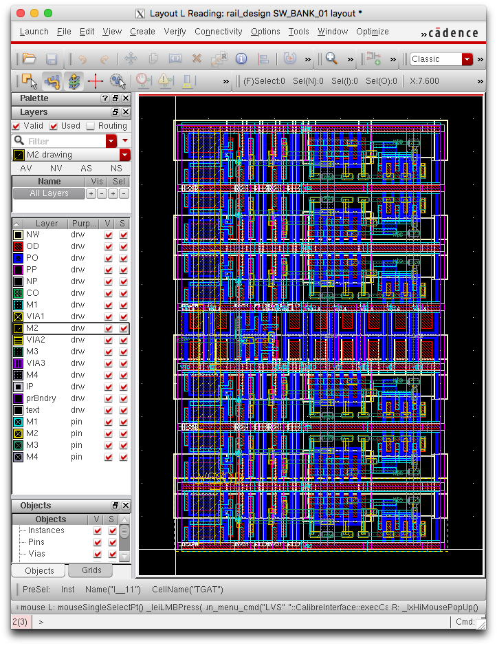
A successful layout import will result in a view as follow,
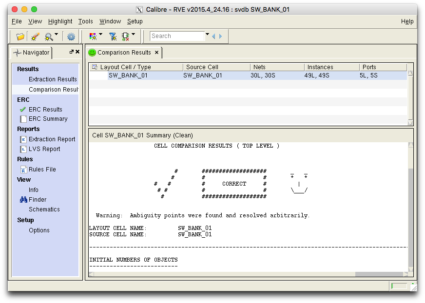
Step 5: RUN the DRC/LVS/PEX and post-simulation
The rest step follows the conventional AMS design follow. We provide a screenshot of the LVS check in calibre below. One of the coolest things in RAIL flow is that the layout it generated is 100% DRC/LVS clean. There is NO worry for unnecessary LVS/DRC debugging in the flow.